22.10.1 D-Script/Global D-Script Restrictions
-
When using external storage, verify the restrictions identified below.
 5.6.3 Restrictions on External Storage Usage
-
In D-Script programming, three addresses occupy the same amount of memory as one Part.
-
The maximum number of addresses you can use in one D-Script is 255. In trigger condition expressions and script programs, read a total of 255 or fewer addresses. Addresses in user-defined functions called into an expression count towards the total number of addresses.
-
D-Script cannot run calculations on floating point values (Float Variables or Real Variables).
You cannot run calculations on structured variables either. However, you can run calculations on individual elements from structure variables.
-
The size of a D-Script affects the Display Scan Time. Note that using a large number of addresses may significantly degrade the program performance.
-
The interval for the trigger bit ON/OFF status or true/false condition must be longer than the communication cycle time*1 or display scan time*2, whichever is longer.
-
Do not specify [Continuous Action], [While Bit is ON], [While Bit is OFF], [While Condition is True], or [While Condition is False] in the Trigger Conditions for the script to write to device/PLC addresses. An error will be displayed because the communication processing cannot keep up with the large amount of write instructions.
To enable these trigger conditions, use the display unit's internal device or temporary address.
-
When there are multiple scripts registered with [While Bit is ON], [While Bit is OFF], [While Condition is True], or [While Condition is False] trigger conditions, and communication with a device/PLC is terminated while the scripts are running, new scripts will not execute. After communication is re-established, the scripts run from the beginning of all the registered scripts.
Even if the process was working on scripts set up on Window screens, after communication is re-established, the scripts restart from the beginning of the Base screen scripts.
-
When calling a function from a function, the maximum number of nested levels is 9. Please do not set up more.
-
Up to 9 levels of nested calls can be created.
-
Up to 254 Functions can be created.
-
When a value is assigned to an address for switching screens while a D-Script command is being executed, the screen switching operation is processed after all D-Scripts have been processed
For example,
ID:00000
Data Format = Bin, Data Length = 16 Bit, Sign = None, Trigger = Bit ON ([b:M0000])
[w:[PLC1]D0100]=0 // (1)
[w:[#INTERNAL]LS0008]=30 // (2) Change to Base Screen 30.
[w:[PLC1]D0101]=1 // (3)
[w:[PLC1]D0102]=2 // (4)
When the above D-Script is executed, processing of the screen switch is performed after (3) and (4) have been processed.
-
When data used in a D-Script is set up with a display unit's touch operation, make sure the data write operation is complete before running the D-script.
-
There is no differenciation between upper and lower case for text in the parameters.
-
In a D-Script or Global D-Script, when using a device address (example: [w16s:[PLC1]D0100]) where you define the access type, the instructions and operators you can use are as follows.
-
Offset Address
-
Addition (+), Subtraction (-), Modulus (%), Multiplication (*), Division (/), and Assignment (=)
[w16s:[PLC1]D0100]=[w16s:[PLC1]D0200]*10%5 //operates normally
[w16s:[PLC1]D0100]=20<<1 //results in an error
if([w16s:[PLC1]D0100]==10) { } //results in an error
memcpy([w16s:[PLC1]D0200],[w16s:[PLC1]D0100],5) //results in an error
-
You cannot use the following characters in folder or file names. as they will cause an error.
: , = + / " [] | < > ? [Space]
-
The following restrictions apply to CF, SD, and USB file operations.
-
You can only use the 8.3 format (8 characters for the file name, the period, and 3 characters for the extension) for the file name.
-
To set a root folder, specify " " (empty string) as the folder name.
-
You cannot use a device address (example: [w16s:[PLC1]D0100]) where you define the access type in the trigger conditions.
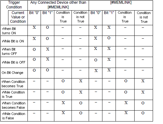
Trigger Condition Operation List When Using Memory Link and Other Devices
Depending on the devices specified for trigger conditions, the D-script operations activated by a trigger after the screen changes or the power is turned on are as follows:

-
When using Global D-Script, the operations mentioned above are performed only when the GP power is turned ON. At the screen change, the above table is not applied, and the trigger conditions are continuously monitored.
-
When the trigger condition in D-script is set to [Timer], a timer starts counting when changing to a screen with a D-script.
-
When the trigger condition in D-script is set to [Timer], a timer starts counting when the display unit is turned on.
Restrictions Specific to Global D-Script
-
Global D-Script operation is suspended during screen changes or other GP operations.
-
After the display unit is turned ON, Global D-Script actions are not performed until all data reads are completed for the initial screen.
After the initial screen changes, Global D-Script actions may be performed before the data reads are completed.
-
The maximum number of devices in the Global D-Script is 255. (Total number of devices used in trigger expressions and script programs.)
When this number is exceeded, the D-Script does not function. Since these devices always read data regardless of the screens, be sure to use only the minimum number of devices required by your D-Script. Otherwise, operation performance can be degraded.
-
The maximum number of Global D-Scripts is 32. The currently used function also counts as one Global D-Script. When the number of Global D-Scripts reaches 32, any subsequent Global D-Scripts are ignored.
Restrictions for SIO Port Operations
-
Addresses designated in the Send/Receive functions are not added to the D-Script address count.
-
The Control is a write-only variable, while Status and Received Data are read-only variables. It you try reading the Control variable or writing data to the Status variable, the operation will not succeed.
-
Create independent D-Scripts (or functions) for Send and Receive operations.
For information about transfer flow charts
 22.5.3.1 Flow Chart
-
The User area in the LS device (LS20 to LS2031 and LS2096 to LS8191) can store data for Send/Receive functions.
-
In the [System Settings] workspace [Script I/O Settings] page, when the [Type] is not set to [D-Script/Global D-Script], the bit 13 in address LS2032 turns ON when the [D-Script/Global D-Script] runs the [SIO Port Operation]'s Label Settings functions (Send, Receive, Control, Read Status, and Receive Data Size).
For information about special relays
 A.1.1.3 Special Relay (Direct Access Method) or A.1.2.3 Special Relay (Memory Link Method)
-
When using the Send/Receive functions, set the bit length of the D-Script to 16 bits. Note that the operation does not work properly if the bit length is set to 32 bits.
-
The size of the Send buffer is 2048 bytes, while the Receive buffer is 8192 bytes. The ER signal (output) RS signal (output) is turned OFF after at least 80% of the Receive buffer is full of received data.
Limitations on BCD Format Operations
If a value which cannot be converted into BCD format is found during operation, the program stops running.
These values include A to F in hexadecimal format.
If the program halts, bit 7 in the display unit's common relay information (LS2032) turns ON. This bit does not turn OFF until the display unit is turned OFF or enters offline mode.
For example,
[w:[PLC1]D0200]=([w:[PLC1]D0300]<<2)+80
If D300 is 3, shifting two bits to the left results in 0x000C, which cannot be converted into BCD format, and interrupts program execution.
[w:[PLC1]D0200]=[w:[PLC1]D0300]<<2
Unlike the above example, 0x000C is the result of the operation to be stored in the memory, and does not cause the program to stop.
Limitations of Zero Operations
If you divide by zero in division (/) and modulus (%) operations, execution will stop. Do not divide by zero.
If the program halts, bit 8 in the display unit's common relay information (LS2032) turns ON. This bit does not turn OFF until the display unit is turned OFF or enters offline mode.
Notes on Delay During Assign Operation
Using a device address in an assign operation may cause write delay because the display unit has to read the address data from the connected device. Consider the following:
For example,
[w:[PLC1]D0200]=[w:[PLC1]D0300]+1 // ...1
[w:[PLC1]D0201]=[w:[PLC1]D0200]+1 // ...2
Statement (1) assigns (D0300+1) into D0200. However, in statement (2), the result of statement (1) has not been assigned in D0200 because of time-consuming communication with the device/PLC. In such cases, program so that the result of statement (1) is stored in the LS area before it is executed, as shown below.
[w:[#INTERNAL]LS0100]=[w:[PLC1]D0300]+1
[w:[PLC1]D0200]=[w:[#INTERNAL]LS0100]
[w:[PLC1]D0201]=[w:[#INTERNAL]LS0100]+1
Notes on dealing with negative numbers
For functions where a negative number is entered for an argument that does not accept negative numbers*3, the entered number operates as unsigned*4.
Cautions When Reading the Same Device Address in the Same D-script
Even when the same device address is used in the same D-script/global D-script, values read from the device address may differ depending on the processing timing of D-script or global D-script.
To avoid this situation, please program scripts to temporarily store data in internal devices or temporary addresses.
Example
When Using Internal Device (USR Area)
[w:[#INTERNAL]USR20000]=[w:[#MEMLINK]0100]
[w:[#INTERNAL]USR00000]=[w:[#INTERNAL]USR20000]
[w:[#INTERNAL]USR00001]=[w:[#INTERNAL]USR20000]
When Using Temporary Address
[t:0000]=[w:[#MEMLINK]0100]
[w:[#INTERNAL]USR00000]=[t:0000]
[w:[#INTERNAL]USR00001]=[t:0000]
![]() 5.6.3 Restrictions on External Storage Usage
5.6.3 Restrictions on External Storage Usage